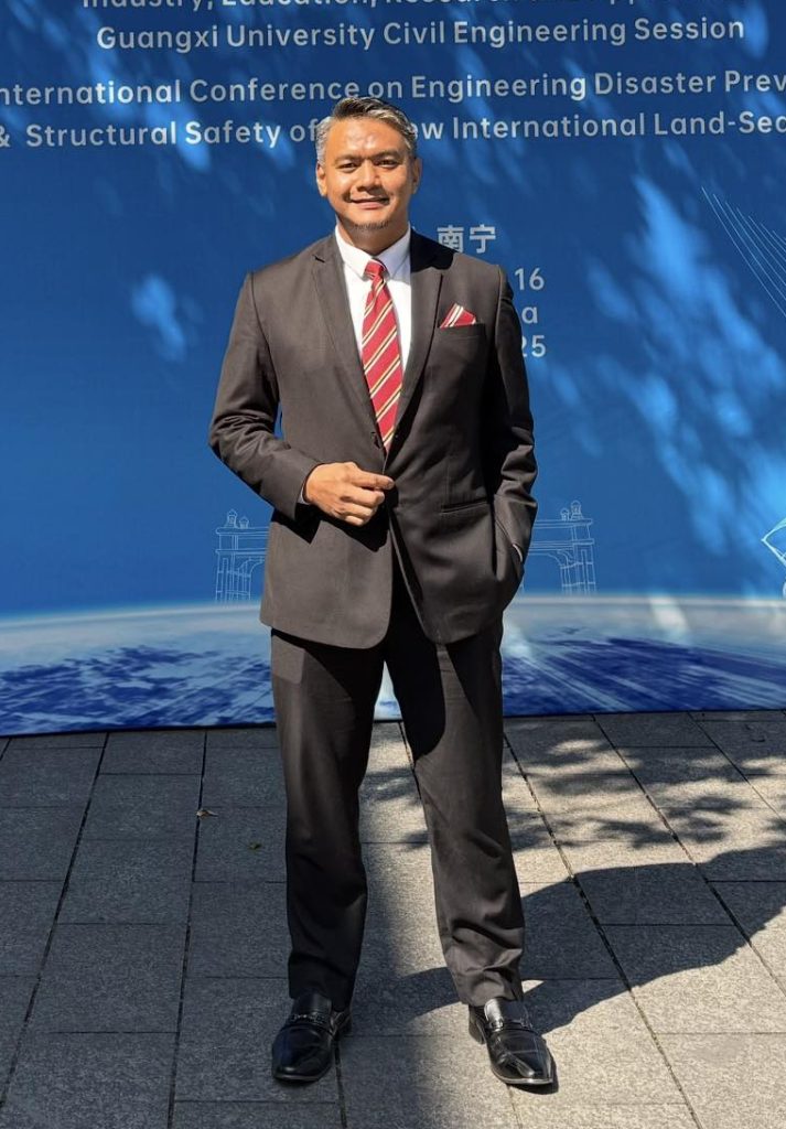
The Journey From Chemor to Tokyo & Oxford
My voyage into electronic engineering started in Chemor, Perak, fueled by an early curiosity to see how minuscule electric currents could instruct massive industrial assemblies. That curiosity became a reality under Malaysia’s Look East Policy, leading me to Japan where I graduated with my Bachelor of Engineering from The University of Tokyo in 1998. Later, backed by the Japanese Government (Monbukagakusho) Scholarship, I completed my Master of Engineering and Doctor of Engineering in Electronics and Information Systems at Gifu University, earning the IEICE Student Research Award and the University Academic Excellence Award. Read my detailed academic qualifications
Before stepping into full-time academia, I spent seven intensive years across the frontline semiconductor manufacturing sector. I began as a Design Engineer at Hitachi Ltd. in Tochigi, Japan, and subsequently worked as a Test Engineer at Unisem (M) Berhad, followed by a Senior R&D Engineer role at STATS ChipPAC. In 2012, I also served as an Academic Researcher at MIMOS Berhad. Those years on cleanroom floors and packaging test cells instilled an uncompromising discipline: an engineering concept is only truly validated when it can survive real-world tolerances, thermal stresses, and high-volume manufacturability. Explore my industrial work experience
In March 2008, I joined Universiti Kebangsaan Malaysia (UKM). Six years into my academic tenure, I was drawn toward healthcare technology, prompting a two-year postdoctoral research appointment (2014–2016) at the Institute of Biomedical Engineering (IBME), University of Oxford, alongside a Research Membership of the Common Room at Kellogg College. There, our team architected digital signal pipelines analyzing photoplethysmogram (PPG) waveforms to detect vital sign abnormalities, deploying digital telemetry systems across clinical health trials in Malawi and South Africa.